Semiconductive Nanostructures - Materials for Spinelectronics
Paata J. Kervalishvili, Georgian Technical University - Tbilisi, Georgia
1. Introduction: nanoscience, nanotechnology and spinelectronics.
Nano spinelectronics, based on usage of magnetic semiconductors, represents new and roughly educing area of science and engineering of the XXI century. The reason to that is the perspective of development and creation of principally new materials and devices for information technologies operating as charge, and spin degree of freedom of carriers, free from limitations inherent for metal spinelectronic devices.
2. Spin – Polarized Transport in Semiconductors.
The essential effort of the scientists are concentrated on studying of the spin-polarized transport in multilayer structures which are including alternating layers of ferromagnetic metals and non-magnetic semiconductors. The central task of such researches is the creation of systems with effective spin injection into a non-magnetic semiconductor. The relevant role in solution of this problem is shunted to search and investigations of new ferromagnetic materials, which are capable to be reliable and good spin injectors. Among such objects the magnetic discrete alloys are very promising. They are multilayer systems composed of submonolayers of a ferromagnetic material in the matrix of a non-magnetic semiconductor, for example, Mn/GaAs or Mn/GaSb. It is well known, that these alloys have high Curie temperatures and sufficiently high spin polarization. The circumstance is not less important that it is possible to control and to manage of the "ferromagnetic metal - semiconductor" boundary surface immediately during the synthesis of these materials.
As it was investigated recently they should be prepared only by the methods of the MOS hydride epitaxy and laser epitaxy with usage of pulsed annealing of epitaxial layers. These technologies are rather simple and, at the same time, allow to perform the doping of layers under the over saturated condition.
Study of the possibility to carry electrons with the spatially oriented spins (the spin transport) from a magnitoactive (ferromagnetic) material in a paramagnetic material represents one of most intensively educing areas of solid-state physics. These applied researches in microelectronics are called as “the spin electronics engineering” or simply “spintronics”. The significance of spintronics is stipulated by perspectives of the development and the creation of new types of a non-volatile memory with random access (MRAM), quantum single-electron logical structures and ultra dense information storage media. Thus, elementary information storage unit will be represented by an electron spin [3,4]. In this case, probably, the limits of the information magnetic recording are reached.
The realization of the spin-polarized current transfer opens out new possibilities for the solid-state electronics also. For instance, there are observations of the spin-polarized luminescence and creation of the high frequency diodes, output characteristics which ones one can change by an external magnetic field [5,6]. Another example is the possibility for creation of a new generation of narrow-band devices of the solid-state electronics of millimeter and submillimeter wave ranges like generators, amplifiers, receivers and filters, modulated and frequency tuned by magnetic field and fully current controlled.
The discovery of giant magnetoresistance effect (GMR) by Fert and colleagues in 1988 [7] can be considered undoubtedly as the beginning of the "Spintronics era". This phenomenon is observed during the study of thin films with alternating layers of ferromagnetic and non-magnetic metals. It is found that, depending on the width of a non-magnetic spacer, there can be a ferromagnetic or antiferromagnetic interaction between magnetic layers, and antiferromagnetic state of magnetic layer can be transformed in ferromagnetic state by an external magnetic field. The spin-dependent scattering of conduction electrons is minimal, causing a small resistance of material, when magnetic moments are aligned in parallel, whereas for antiparallel orientation of magnetic moments the situation is inversed. The effect GMR brightly has demonstrated, that a spin-polarized electrons can carry magnetic moment through non-magnetic materials with saving spin coherence, this is the meaning of the term “spin transport” nowadays.
Namely the GMR effect was used in a new generation of the magnetic field sensors, which appeared in 1994 as commercial products on market. But present boom in industry producing the information storage devices started a bit later, in 1997, when the IBM Company has presented the first hard drives with the GMR reading heads. The implantation of this technology has allowed more than on the order to increase a density of the information storage on magnetic disks, and the size of the market of these reading heads already exceeds 1 billion US dollars.
The sensors operating with the tunnel magnetic junctions (MTJ) fall into the second class spintronics devices.There ferromagnetic electrodes are divided by very thin dielectric layer, and electrons are tunneling through a nonconducting barrier under influence of applied voltage. The tunnel conductivity depends on relative orientation of the electrode magnetizations, and tunnel magnetoresistance (TMR) it is small for parallel alignment of magnetizations of electrodes and is high in opposite case. In contrast with the GMR of devices, electrodes are magnetic independent in this case and have different critical fields for changing of the magnetic moment orientation. The first laboratory samples of (NiFe/Al2O3/Co) MTJ structures were demonstrated by Modera and colleagues in 1995 [8], where the TMR effect reached 12 % at room temperature.
Some largest manufacturers of an electron technology, including the IBM Company, have declared recently about the development of new in essence memory devices: so-called MRAM [9]. They include storage units based on the MTJ structures and allow not only to increase essentially the storage density and the access speed to a memory, but also to provide complete saving of data at disconnecting of a power supply. The first industrial designs of such memory devices have appeared already in 2003 in the commercial market. A disadvantage of these devices is the small scale of integration, bound with necessity of usage of additional controlling transistors. Possibility to overcome these limitations is connected nowadays only with the development of the semiconducting spintronics, and, in particular, with the creation of spin transistors. In this case spintronic devices can not only switch or to detect electrical and optical signals, but also to enhance them, and also to be used as multifunction units. Only in this case spintronic devices can not only switch or detect electrical and optical signals, but to enhance them and can be used as multifunction units.
Due to this reason, the third direction of development spintronic devices is based on the development of multilayer nano structures of ferromagnetic semiconductors, which demonstrate properties not available for their metal analogs. One can refer to number of these properties the possibility to control by electric field a magnetic state of material [10] and the giant planar Hall effect, which exceeds on several orders of magnitude the Hall effect in metal ferromagnets. The super-giant TMR effect observed for the first time in epitaxial (Ga,Mn)As/GaAs/(Ga,Mn)As structures [11] is not less promising for applications.
Surprisingly, but the development of spintronics in the ХХ century drove practically irrespective from the semiconductors technology. Naturally, that the association of these two directions is extremely necessary with the purpose to combine well controlled electronic properties inherent for semiconductors with additional possibilities of devices; in which the spin degree of freedom of current carriers is used. Namely this represents the essence of the semiconducting spintronics, and its central problem is today the search of an effective way for the spin injection in a semiconductor from the spin-polarized reservoir.
There are no effective ways of injection the spin-polarized current in non-magnetic semiconductors at the present moment, [12,13]. The spin injection from magnetic semiconductors in non-magnetic gives good results in a number of cases [14], but while it has a place only at low temperatures, far from room temperature.
So-called magnetic discrete alloys [15, 16] to days are of the most prospective materials for solution of the spin injection problem. These alloys involve a periodic system of sub-monolayers of magnetic ions (for example, Mn), placed between semiconducting layers (GaAs, GaSb, InAs) forming a magnetic superlattice. There are as incidentally distributed Mn ions and 2D magnetic islands of MnAs (or MnSb) as well in manganese containing layers. The discrete alloys have high Curie temperatures (above 300 K for the GaSb-system), demonstrate extraordinary Hall effect at high temperatures [15, 16] and have a relatively high degree of the spin polarization. It is possible in such systems to control not only quality of the border "ferromagnetic metal - non-magnetic semiconductor", but also manage of the current carrier’s concentration and change the type of magnetic ordering. The discrete alloys should be considered as random magnet systems owing to hardly inhomogeneous allocation of a magnetic phase in sub-monolayers.
3. Nanostructures of wide forbidden zone semiconductors.
High-temperature semiconductors with wide forbidden zones are also the very promisable materials for modern nano electronics. Materials based on carbon and boron provide complicated substances with unique structural properties. The technology for their film preparation is promising with their desirable electric and physical properties such as mechanical hardness and chemical resistance. Research conducted during the last decades of the 20th century have shown that carbon and boron crystals form clusters, the essential structural elements of which contain 4, 12, 60, or 84 atoms. These nanoelements, due to their thermodynamic properties, transform to amorphous or crystalline films, layers and other deposits, which have some advanced properties.
The clusters having a stable configuration under equilibration conditions take the forms of different geometrical figures - from triangular to dodecahedral and icosahedrical [17,18].
According to the classical idea of particle formation and growth and in correspondence with the so-called atomistic process of conception, atoms being the germ of the solid phase unite in aggregates (clusters) where their quantity is dependent on their atomic potentials.
Statistical calculations of the thermodynamic properties of small clusters carried out by means of computer modelling have shown that the potential energy of the atomic cluster components is the main factor determining the chemical potential of the cluster.
The elemental atoms in small aggregates can be packed according to the laws of crystallography together with that of non-crystallographic pentagonal symmetry. However, the pentagonal symmetry of clusters despite its small deviation from crystallographic packing is energetically less advantageous. This becomes partially apparent when the crystal growth in the complex is accompanied by the corresponding increase in inter-atomic space.
The growth in the quantity N of atoms in the cluster results in the increase of the thermodynamic potential P (N), caused by the increase in atoms at the surface. At the same time, the increase of surface energy accompanying the additional atoms is not continuous, but discrete because of the differences between the energetic contributions of the atoms completing the formation of the co-ordinating sphere [19].
Further growth in the aggregate [20,21] leads an increase in the volume by means of a gradual addition of atoms from the sides to the growing cluster - volume growth. Using the established and recent approach to the mechanism of cluster formation, it is easy to show that the appearance of small particles analogous to the so-called fractal clusters very often takes place. Following this, the particle growth occurs not by the joining of separate atoms to their existing aggregate, but by a conglomeration of aggregates with stable configuration, which preserves their individual properties. Such volume clusters consisting of separate clusters of lesser dimensions have much lower density than the matrix substance. Often they are the simplest structural elements (tetrahedrons, cubes, bi-piramides, etc.), one or some surface parts of which are stuck together.
The formation of small particles (clusters) is actually carried out by various methods, among which are supersonic outflow of vapours into the vacuum, thermo-, laser- and plasma-chemical modes of substance reduction from their gas-phase compounds, vapour precipitation upon cold substrates, reaction of molecular effusion from a cell, and etc. These techniques are being used to study the process of the small particle formation, volume growth and growth on specially prepared surfaces.
The production of elementary boron is presently being developed by various powder and film technologies [22]. The greatest interest is with modes of small particle production to provide high dispersion and purity as well as the study of the processes of cluster conception and growth.
Established theory and experiment have shown that the elementary boron atoms group into an aggregate of icosahedrical form consisting of 12 boron atoms (B12) [23,24]. Usually the boron small particles consist of one or more icosahedrons united in a cluster or various configurations depending on the thermodynamic conditions at formation.
Designating the chemical potential of the structural element (in boron this is a 12-atom icosahedron, in carbon it is a 4-atoms tetrahedron) as E, and the chemical potential of the flat particles (cluster) as P, it is apparent that an equilibrium between the longitudinal dimensions and flat cluster thickness will be achieved when ![]() E -
E - ![]() P = 2av/r, where a is the surface specific free energy per one structural element, v is the specific volume of cluster per one structural element (this is analogous to the Gibbs-Thomson expression), r - radius vector . Given that the equilibrium form is subordinated to the second order non-linear differential equation[25,26] and the difference
P = 2av/r, where a is the surface specific free energy per one structural element, v is the specific volume of cluster per one structural element (this is analogous to the Gibbs-Thomson expression), r - radius vector . Given that the equilibrium form is subordinated to the second order non-linear differential equation[25,26] and the difference ![]() E -
E - ![]() P is constant over the whole surface of a particle, the solution of this equation represents the envelope of the cluster:
P is constant over the whole surface of a particle, the solution of this equation represents the envelope of the cluster:
![]()
![]() = 2a (
= 2a (![]() ) n /(
) n /(![]() E -
E - ![]() P)
P)
where ![]() is the vector of the normal to the envelope ( the surface) of the small particle as determined by the radius vector
is the vector of the normal to the envelope ( the surface) of the small particle as determined by the radius vector ![]() = r (the expression is analogous to the Curie-Wulf formula [27]). From this equation it is possible to evaluate the geometric form and longitudinal dimension of the equilibrium state of the cluster of elementary boron in flat form (fig.1) under given thermodynamic conditions.
= r (the expression is analogous to the Curie-Wulf formula [27]). From this equation it is possible to evaluate the geometric form and longitudinal dimension of the equilibrium state of the cluster of elementary boron in flat form (fig.1) under given thermodynamic conditions.
Fig.1 - Schematic picture of a cluster of 12 - atom icosahedrons in plane form
During electron-microscopic studies and testing of the structure of elementary boron produced by means of boron three-chloride reduction with hydrogen and laser-chemical multi-photon dissociation of the dichlorboran molecule, the observed structural elements - boron icosahedrons, are statistically disseminated in an amorphous condition and in a crystalline condition with rhombohedric symmetry.
Investigation and testing was conducted with light-permissible electron microscopy (HEM) EM-100/OR “OPTON”. The study used free-poured ultra-dispersed amorphous boron powder [27] produced by plasma-chemical reduction of boron three-chloride with hydrogen.
During the electron-microscopic study with the electrons acceleration voltage of 100 kV, light-permissible pictures were produced with microscopic magnification 2 ´ 10-5. The additional phase displacement caused by spherical aberration between non-dispersed and diffracted beams defocused the pictures but was compensated by the defocusing of the lens. Under the Schercer focus, the particularities of the initial structure of the specimen and its alteration under thermal absorption of the electron beam as well as under the thermal treatment of the particles in deep vacuum were observed. The electron microscopy picture shows that the particle has an amorphous structure, boron icosahedrons are placed non-regularly in the plane.
The analysis of the micro-diffractional picture, consisting of three diffusion halos, as well as calculations of the interplane spaces has given values consistent with those for the planes of the icosahedron B12. A number of boron particles partly overlapping each other is shown in fig.2. The particles form plane structures with longitudinal dimension 20-40 times as large as their thickness. The thickness is approximately equal to the linear size of 12-atoms of boron.
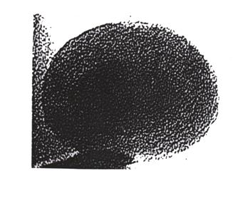
Fig. 2 - Electron microphotograph of boron particles which are overlapping each other
Thermal treatment of the boron powder in a vacuum 1×10⁻⁶ Pa at a temperature of 800° C and for a period of 30 min. leads to the partial crystallization of the internal particle spheres (stripe contrast, typical of crystalline condition) while round these spheres an amorphous structure is preserved. The analysis of the analogous electron microphotographs shows that the increase of the longitudinal dimensions of the particles under the thermal treatment occurs because of the joining of lammelar clusters formed from boron icosahedrons with the initial dimension 2-5 nm and icosahedron thickness, and because of their stratification.
The space between the normal stripes is 0,8 nm, which is very near to the interplane space of planes (111) of b - rhombohedrical boron (d111 =0,7962 nm) in crystalline structure and coincides with values calculated from interreflex space data.
Thus, the direct observation of small particles of elementary boron using high-permissible electron microscopy shows that the boron clusters (2-5 nm) are the amorphous plane compounds where the ratio of the thickness to the longitudinal dimension varies from 1:10 to 1:40. These clusters which consist of non-regularly thermally treated small particles of boron proceed to crystallisation, which at first occurs in the centre of a particle without its plane structure, then advances to the stage of a partly crystallized clusters, stratification and finally volume crystallisation.
The elementary particles of boron produced by the plasma-chemical method in the free-poured state have shown an unknown effect – the appearance of a plant-shape cluster [28,29]. In other words, the ultra-dispersive amorphous boron powder clusters consisting of statistically (nonregular) distributed icosahedrons has been found. These clusters have an elliptic or ellipsoidal configuration and longitudinal dimensions the value of which is some tens time the diameter of the structural element B12 .
The thermal treatment of the elementary boron powder, which consists of plane clusters, in a vacuum furnace as well as in the electron microscope’s beam resulted at first in a transition of icosahedrons from a statistical into a modulated condition and then their grouping into a volume rhombohedrical configuration of crystalline boron of b -type. At the first stage there has been observed a regulation of the icosahedrons in the flat form (fig.3), and then at the second stage a unification of these forms accompanied by the crystalline phase formation. The revealing of elementary boron structural elements in flat clusters characterised only by the near order is direct experimental corroboration of the energetic advantage of the existence of small particles with a flat geometry and of the existence of spaces during the growth of solids from atoms to a cluster and further to a massive specimen in which the solid substance appears as a flat micro-formation consisting of statistically distributed structural elements (in the case of boron these elements are icosahedrons).
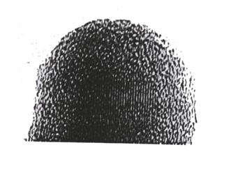
Fig. 3 - Electron microphotograph of a small particle of boron at the first stage of regulation
Similar results were observed in the case of ultra-dispersive carbon powders. The electron microscope studies show that the carbon powder consists of small structural elements in the forms of tetrahedral disks. On receipt of a very small portion of energy they organized into the bigger clusters, sometimes the so-called Fullerenes. In the electron microscope beam after treatment they become crystalline structures and in suitable thermodynamic conditions, become diamond.
The same situation occurs with carbon layers prepared by the laser spraying - laser plasma technologies [30].
The Laser Spraying Method for film and layer preparation and its most attractive and advanced development, Laser Plasma Deposition, was used for boron and carbon thin film and layer production (fig.4). The laser beam is focused on the target placed in the vacuum chamber. The films are deposited on the heated substrates with the temperature varied in the range of 300 – 1300 K. Plates of crystalline boron and carbon (graphite) were used as a target. The energy source may be the repetitive pulsed, continuous as well as the other types of laser. These technologies are rather simple but allow the doping of layers under the over saturated condition.
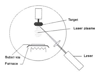
Fig. 4 - Schematic diagram of the Laser Plasma deposition method
Investigations have shown that the prepared crystalline layers have a diamond like structure with the lattice parameters close to that of crystalline diamond [31].
Further study of small particles, their conception and growth will explain a number of natural phenomenon of the formation of small solid structures.
The practical importance of this investigation consists of the possibility to create new technologies for the production of ultra-dispersive materials with given crystalline or amorphous structure and the requisite properties [32,33]. Recent experimental studies of small solids - particles, structural elements of some non-organic (carbon, cobalt, etc.) and biological systems (biomolecules, bio-solids) have brought new data regarding the nature of the kinetics of their formation.
REFERENCES
- J.J Ramsden, Nanotechnology Perseptions. Vol.1, N 1 (2005) pp.3-17.
- P.J. Kervalishvili, Proceedings of the International Conference on Materials Testing, AMA -Nuremberg, 13-15 May 2003, pp.107-112.
- D.D. Awschalom, M.E. Flatte and Nitin Samarth, Scientific American, June (2002) p 27.
- G.A Prinz., Physics Today, 48 (1995) p 353.
- R Flederling., M. Kelm, G. Reuseher Et al., Nature 402 (1999) p.787.
- Y. Ohno, K.Young, B. Beschoten Et al., Nature 402 (1999) p 790.
- M. Baibich, J. Broto, A. Fert, F.V. Dau, F.Petroff, P. Etienne, G. Creuzet, A. Freiedrich and J. Chazelas, Phes. Rev. Lett. 61 (1988) p 2472.
- J.S. Moodera, L.R. Kinder, T.M. Wong and R. Meservey, Phys. Rev. Lett. 74 (1995) p 3273
- S.S. Parkin, K.P. Roche, M.G. Samant, P.M. Rice, R.B. Beyers, R.E. Scheuerlein, E.J. O'Sullivan, S.L. Brown, D.W. Abraham et al, J.Appl. Phys. 85 (1999) p 5828.
- S. A.Wolf et al., Science 294 (2001) p 1488.
- C. Ruster, C. Gould, T. Jungwirth, J. Sinova, G.M. Schott, R. Giraud, K. Brunner, G. Schmidt and L.W. Molenkamp, Сond-mat/0408532 vo1, 25, 2004 p 234.
- Spin Electronics, ed. By M. Ziese, M. J. Thornton. (Springer-Verlag, Berlin, Heidelberg, (2001).
- G. Schmidt, L.W. Molenkamp (review), Semicond. Sci. Technol. 17 (2002) p 310.
- B. Jonker, et al., Phys. Rev. B 62 (2000) p 8180.
- X. Chen, et.al., Appl. Phys. Lett. 81 (2002) p 511.
- B. D. McCombe, et al., Physica E 16 (2003) p 90.
- U.T. Petrov, Small Particles Physics, Nauka, Moscow, 1982, p. 356.
- R. Kern, The equilibrium form of a crystal, Morphology of Crystals, ed. I. Sunagawa, Terra, Tokyo, 1987, pp. 77- 206.
- V.K. Vainshtein, A.A. Chernov, L.A. Shuvalov, Up-to-day Crystallography, v.B - Formation of crystals, Nauka, Moscow, 1980, p. 408.
- H.Brune, H. Roder, C. Bogarno, K.Kern, Microscopic View of Nucleation on Surfaces, Phys. Rev. lett., v. 73, 1994, pp. 1955-1958.
- P. Kervalishvili, T. Jandieri, Proceedings of the Ac. Sci. USSR, Inorganic Materials, Vol.27, N7, (1986) p 1115.
- Boron and Refractory Bodies. Ed. by V. Matckovich, Berlin-Heidelberg, Springen-Verlag, 1977, p. 485.
- 9. W.N. Linpscomb, Borides and Borates, Journal of Less-Common Metals, v. 82, 1981, p. 1-20.
- G. Abdushelishvili, T. Abzianidze, P. Kervalishvili, Laser Chemistry, Vol.10,(1989) p 81.
- 11. L. Landau, V. Lifshits, Statistic Physics, part 1, Nauka, Moscow, 1975, p.584
- J. Bernholc, E.L. Briggs, M. Buongiorno Nardelli et al. In book Multyscale computational methods in chemistry and physics. Ed by A. Brandt et al. IOS Press, 2001, pp. 65-89.
- .P.J. Kervalishvili, Solid State Physics, v. 28, N 12, 1986, p. 3218-3220.
- P.J. Kervalishvili, E.R. Kutelia, V.S. Petrov, Electron-microscopic Structure of Amorphous Boron, Solid’s physics, v. 27, N 5, 1985, p. 1414-1418.
- P. Kervalishvili. Some investigations of small particles growth. XIV PanHellenic conference on physics. Ioannina-Athens, 1998, pp.75-88.
- P. Kervalishvili, S Shalamberidze, G. Esadze. Thin films preparation by Laser-Plasma deposition. Le vide, les Couches Minces. N 267, Mai-Juin-Juillet 1993, pp. 186-197.
- A. Gippius. Semiconducting diamond: properties and applications. Proceedings of the X PanHellenic conference on physics, Delphi –Athens. 1994, pp. 54-59.
- Ch. Lieber Proceedings of
- P. Kervalishvili. S. Shalamberidze, Yu. Bikovski. AIP Conference Proceedings. Vol.231, N1 (1991) p 524.